Category: Technology

27 Jun 2023
AP Master Nozzle

AP Master Nozzle FAQ’s

AP Master Nozzle FAQ’s

Authored By: Dr. Samuel J. McMaster: [email protected]

Materials Scientist at Pillarhouse International Ltd.


The AP Master Nozzle represents a dramatic leap forward in nozzle performance, offering both improved lifetime and wetting. As these nozzles are now available, you may have questions about how they will fit in with your current soldering platform. This Q&A document will cover the most commonly asked questions about the AP Master Nozzle.

What features can be expected with the new AP Master Nozzle?

  • Better initial wetting for faster start-up of the nozzle and more user-friendly operation.
  • Innovative surface treatment improves long-term wetting and wear performance.
  • Lifetime predicted to be at least 8 times longer than a standard AP nozzle.
  • Surface treatment resists oxidation at high temperatures allowing for easier rewetting of the nozzle.
  • Better pull-off performance enables soldering of fine-pitch components.
  • Compatible with all current solders and fluxes on the market.
  • Compatible with the current Pillarhouse nozzle mounting system.
  • Available exclusively on all Pillarhouse machines using wettable nozzles.

What nozzles will be available in the new AP Master design?

All wetting nozzles will be available in the new design. This will encompass our AP, Jet Tip, Extended AP, Extended Jet Tip, and Micro Nozzles. The Wide Wave and Jet Wave apparatuses do not wet the solder and therefore remain unchanged. However, the wetted plates will utilise the new material design to improve their lifetime.

Is there any change in the mounting system?

No, so long as you are using the current external thread option (see Accessories & Spares brochure) you will be able to install the new nozzle into your soldering system. We will no longer be producing the mounting hardware for the internal thread system. If you are still using this system, please contact Pillarhouse and we will arrange a free-of-charge swap to the new mounting system.

Will the nozzles be available using the magnetic mounting system?

Yes, the nozzle can be made available for the magnetic mounting system, however, we always recommend threaded mounting as it is more secure.

Do I need to use different fluxes with the AP Master Nozzle?

No, the nozzle is compatible with all the current fluxes on the market. Pillarhouse continues to recommend the use of Activ8 to clean and tin the nozzles for manual cleaning. The adipic acid used in the auto tinning module will also be effective for maintaining the wetting of the solder to the nozzle.

The surface treatment applied to the nozzles increases the wettability and increases the resistance to oxidation, but maintenance must still be conducted and soldering in an inert atmosphere is essential.

Is there any difference in the wetting between the AP Master Nozzle and the original AP Nozzle?

The wettability of the AP Master Nozzle is greater than the original AP Nozzle. This allows for faster initial start-up of the nozzle, easier rewetting of the nozzle and soldering of finer pitch components. Wettability and spreading of the solder will always be poor in an oxygen-rich environment due to the oxide film that grows on both the solder and nozzle therefore nitrogen must still be used to inert the environment around the nozzle.

What lifetime can be expected with the AP Master Nozzle?

With the correct maintenance, the AP Master Nozzle will last at least 8 times that of the original AP Nozzle. On average, the original AP Nozzle (in 6 mm form) will last 213 hours. Therefore, the lifetime of the new nozzle will be approximately 1,700 hours. This estimate is based on ideal circumstances and can be affected by more corrosive solders, more extreme soldering processes, and poor maintenance.

How do I maintain the AP Master Nozzle?

Using the same methods as with the original AP Nozzles. Liquid flux should be used for manual cleaning. Abrasive cleaning can be used as with the original AP Nozzles, but this will remove more material from the nozzle and will decrease the overall lifetime; this should only be employed in extreme circumstances for dewetting issues. Overall, the same maintenance schedule should be followed as recommended by Pillarhouse.

How can I order the new AP Master Nozzle?

You can order the new AP Master Nozzle either directly from Pillarhouse or from our agents, as of right now. The new design will replace all our existing wetting nozzles from this time and all shapes will be available with the same part numbers as with the old design.


For more information on Pillarhouse International’s AP Master Nozzle, read here: Selective Soldering: A Need For Innovation and Development (pillarhouse.co.uk)

09 Jun 2023

Selective Soldering Challenges and Meeting Training Needs

Selective Soldering Challenges and Meeting Training Needs

Authored By: Dr. Samuel J. McMaster*1,2, Kane F. Witham*1, Professor Andrew Cobley*2, Dr. John E. Graves*2, Eddie Groves*3

1 – Pillarhouse International Ltd., Rodney Way, Chelmsford, CM1 3BY, UK

2 – Functional Materials and Chemistry Research Group, Research Centre for Manufacturing and Materials, Institute of Clean Growth and Future Mobility, Coventry University, Priory Street, Coventry CV1 5FB, UK

3 – Selective Soldering Academy, 201 Lively Blvd, Elk Grove Village, IL 60007


1.     Introduction

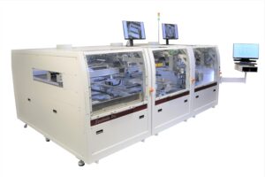
Selective soldering has grown in popularity over the past 25 years to now be a major connective technology in the electronics industry. The machines and techniques have progressed to being a major feature of in-line processes with the ability to flux, pre-heat[1] and solder through-hole technology (THT) components for printed circuit boards (PCBs) within a single machine or series of modular machines. As described by McMaster et al. [1], there are 2 classes of selective soldering machines: hand-load and in-line machines. As in-line systems are used for processing either a greater volume of boards or larger boards, many of the most challenging selective soldering processes are undertaken with this equipment.

[1] Typically fluxing will be applied before pre-heating for PCB solder processing so that the temperature of the pre-heat step can activate the flux.

2.     Challenges in selective soldering

Broadly, the challenges in selective soldering can be described as fitting into two main categories. The first of which is process requirements wherein a particular printed circuit board must be processed within a specific timeframe to meet the defined production schedule. The second of the challenges is the soldering of boards with increasing complexity of design, large amounts of surface mount components and high thermal mass. The following sections will discuss each of these challenges in more detail.

2.1. Process challenges

Multiple elements make up a selective soldering process [2]. The first of which is generally the fluxing step. Fluxing fulfils several purposes for the selective soldering process:

  • Creating a film between the solder mask and the solder to avoid the adherence of solder to the PCB.
  • Cleaning the metal surfaces of components to remove oxides to make soldering possible.
  • Promotes the wetting of the solder for better hole fill.
  • Aids in the prevention of solder bridges and solder balls.

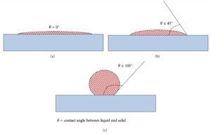
There is no one size fits all flux; they can be alcohol-based, water-based or rosin based. Solid content can vary as can the active chemistry. Application methods can vary depending upon the process requirements but generally, two methods are used. The drop-jet can quickly apply miniature droplets in a precise fashion. Water and alcohol-based fluxes can be used with the drop-jet. When a larger area is to be soldered, an ultrasonic head is used. This fluxing module is lower maintenance and can handle higher solids content fluxes.

After fluxing, the board would generally be pre-heated. This activates the chemistry and prepares the board to better wet the applied solder. Most commonly, infrared (IR) lamps are used with a wavelength between 750 nm and 3000 nm. Balancing the wavelength of the IR with the absorption of heat of the parts is key. IR can quickly respond (1-3 seconds) to heat the board and can be used in closed loop mode (taking a temperature reading and altering the power to hit a desired thermal profile) or open loop (where the lamps simply heat the assembly without imposed power control)

For thicker boards, convection heating may be used. This technology is slower to respond than IR resulting in pre-heating steps in the range of multiple minutes compared to 1-2 minutes for IR. Convection is, however, able to evenly heat thicker PCBs and isn’t bound by the reflectivity issue of different wavelengths of IR lamps.

To achieve the optimal pre-heating for a specific product, a thermal profiler should be used to determine the maximum temperature, thermal ramp rate and pre-heating time. For some processes, the PCB is then enough that pre-heating doesn’t need to be used and the heating from the applied solder is enough. The order of fluxing and pre-heating can be changed depending on the process requirements for the board and depending upon the flux being used. As heating is applied to the board, a water-based flux will spread whereas an alcohol-based flux will begin to evaporate. Proper process engineering ensures that the order and timings of these processes are specified.

Following these steps, it’s finally time for soldering. As with all the other elements of the selective process, there are multiple parameters and options to consider during this step:

  • Inertion: To maintain good flow characteristics and reduce the amount of bridging, a low-oxygen environment is used. Nitrogen is typically used for inertion to achieve sub 10 ppm of oxygen. 50 ppm of oxygen is the maximum permissible limit, above this the solder quality is affected and dross is generated at a higher rate.
  • Positioning of the solder bath[2]: The bath positioning can be used to either apply soldering to a single joint or closely packed series of joints in a dip step or movement along the underside of a PCB. The machine can be programmed for rows of connectors as part of a draw step.
  • Contact time of solder: Greater contact time can aid wetting and pull-through of solder but increasing the time can dissolve copper from the PCB.
  • Type of solder: lead-free or leaded; inclusion of additives to alter the liquid properties or the mechanical properties of the solidified joint.
  • Use of wetting or non-wetting nozzles: non-wetting dip nozzles can be used for fast production of high-volume products, but they lose the per-joint customisation of a wetting nozzle.
  • Top-side heating during soldering: used if the assembly has a high thermal mass that required continuous heating to ensure good solder pull-through.
  • Solder temperature: The soldering temperature is chosen to balance good pull-through, flux activation loss and increased likelihood of oxidation. Generally, the temperature will be in the range of 280-320 °C.
  • Board warp correction: the application of heat to the PCB can warp it enough to affect the soldering process. The use of a laser positioning sensor can apply live offsets to the programmed height to achieve good soldering.
[2] Pillarhouse typically employs a fixed PCB during soldering with a moving soldering bath and nozzle.

Nozzle size and type can be customised for specific joints but there correct programming must still be utilised as there are so many parameters that interact to produce a well-soldered joint. With new materials engineering, the maintenance can be reduced as with the AP Master nozzles [3,4]. The increased wetting enabled by surface engineering technologies allows for faster start-up of the nozzles, easier rewetting and less dewetting during process. Cleaning is still essential to keep a nozzle running well no matter the material design[3].

[3] Nozzles are also cleaned with flux however a different chemistry is utilized to remove the oxides that form on the surface of the ferrous materials utilized as nozzles.

A unique item that poses a challenge is not, in fact, an issue of process technology but is more people-centred. No one likes doing maintenance, but it is essential to keep all machines working properly. Machine wear out is inevitable. Proactive maintenance is undoubtedly better for a full production environment but this is more time intensive and requires greater planning [5].

Sometimes nozzle sizes are chosen to fulfil the requirements of multiple products. In this case, it is often more optimal to use planned machine downtime to swap to a different nozzle size to produce better soldering quality. This takes more time and planning from maintenance staff, however. Some customers will opt to use a heated bath trolley to allow for faster changing of baths (to use different solders or a different nozzle geometry). The heating function also allows maintenance to be carried out of the baths outside of the soldering system; when the bath cools the impeller chamber is frozen, so it is inaccessible.

Finally, electronics manufacturing is becoming increasingly automated, and the soldering systems must be adapted to fully integrate with this new paradigm of manufacturing. Examples include the use of robot arms to load PCBs into the machines, re-soldering in in-line soldering machines based on optical inspection results and automated nozzle conditioning and solder top-up systems.

2.2. Board-specific challenges

Often Pillarhouse engineers will encounter PCBs where little consideration has been given to the end manufacture process. As selective soldering will be viewed as the last element of the manufacturing chain, it is the last thing a design team may think about. Furthermore, many design teams may not be experienced with optimal design elements to enable fast processing with selective soldering. Often extended nozzles need to be used to work around tall components. Additionally, customers will approach Pillarhouse with boards that were built with surface mount technology (SMT) assembly in mind necessitating the use of smaller nozzles with more precise programming.

With the rapid increase in electric vehicle systems, there has been an increase in PCBs bonded to larger cooling assemblies which pose a challenge in terms of pre-heat as well as soldering larger components such as insulated-gate bipolar transistors (IGBTs).

These board-specific challenges require careful setting of process parameters to ensure good soldering within the time requirements. This involves setting the pump speed to achieve the correct level of solder fill and ensuring the nozzle remains wetted, programming the optimal vectoring of the solder bath and pull-off characteristics to reduce bridging.

3.     The Selective Soldering Academy (SSA)

Due to the level of adoption of selective soldering technologies and their importance in the circuit board assembly process, it’s now more likely that you will find more assembly facilities with it than without[6]. To be able to maintain and run a selective soldering machine and overcome the challenges described above, training is essential.

The SSA exists to train anyone (not just those with Pillarhouse equipment) on the correct practices for running equipment, maintenance and how to approach programming new boards to enable customers to set up new processes quickly, keep them running and maximise the financial impact of the selective soldering process.

4.     The SSA Challenge Board

The main teaching element of the SSA is the Challenge board. It’s unlikely that a real-world soldering process will possess all the elements in this PCB; function is not the aim of this board, it is designed to be difficult to solder and it’s impossible to successfully solder all elements with one type of nozzle.

The board is 0.075” (1.91 mm) thick with 4.2 oz (56.7 g) copper layers. Two of the layers are ground planes while the other two have only traces. Some connections to the ground planes are heat relieved.

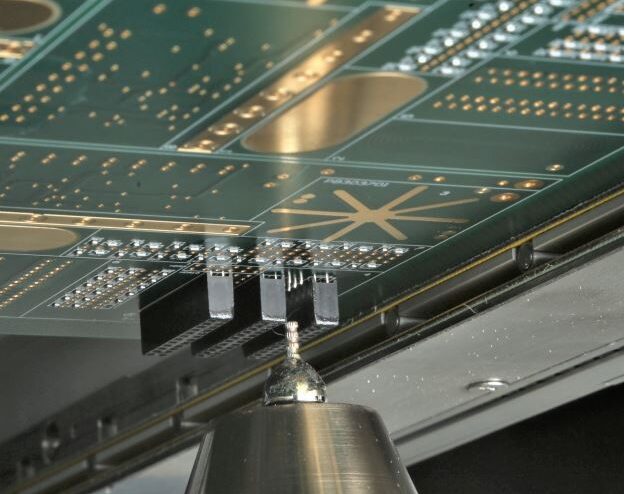
Silkscreen is used to partition each area of the board and each section is numbered to help identify the specific techniques to be used in each. SMT and THT are on both the board’s top and bottom sides. Figure 1 shows the bottom-side of the PCB which is the starting point for THT soldering.

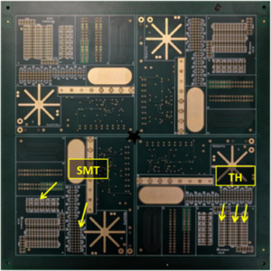
Figure 1. Bottom-side view of the SSA Challenge board.

Figure 2 shows the top side of the PCB. Unlike the bottom-side, the top-side SMT and some nearby THT parts are functional and are highlighted in yellow. This is part of the surface insulation resistance (SIR) test area. There is also a simulated SIR coupon to be soldered to the board in the green highlighted area.

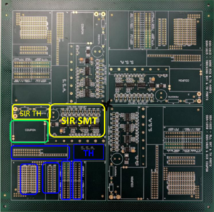
Figure 2. Top-side view of the SSA Challenge board.

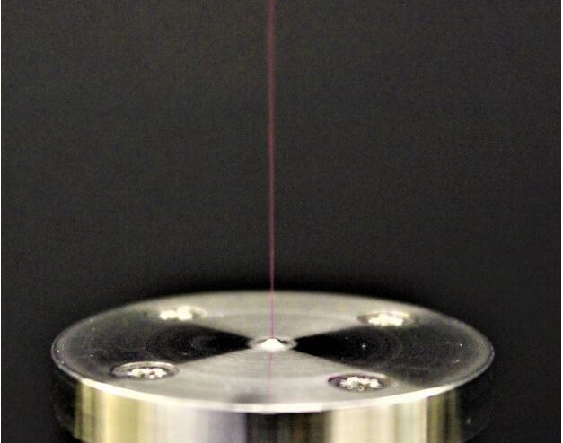
Figure 3 shows a close-up image of one of the test areas on the bottom-side of the board. The red highlighted areas are for practising soldering using the micro-nozzle allowing you to solder near metallised areas or SMT components. The blue area is to test the effectiveness of fluxes for solder spreading; the cross pattern is used to highlight the spreading further. The yellow area is to test the wetting performance of flux on a bare metal finish. A solder draw can be programmed on this area to observe solder wetting and spreading. Finally, the green area is used to observe flux wetting on solder mask.

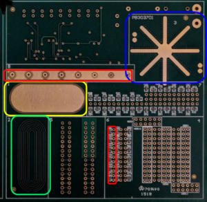
Figure 3. Closeup of solder and flux test areas.

5.     Conclusions and future developments

Selective soldering has now reached a stage of maturity where it can be considered its own processing technology. As a result of this, PCBs should be designed with this processing technology in mind however the innovations in selective soldering (e.g., the micro-nozzle) can mitigate against designs where this is not possible. Experienced and knowledgeable staff will be able to program process conditions to maximise the potential of selective soldering. Emerging markets such as electric vehicles have shown that selective soldering technologies continue to grow in popularity. The AP Master Nozzle technology will enable increased soldering capabilities and easier maintenance of wettable nozzles to help meet the demands of growing markets.

For more information on Pillarhouse International’s AP Master Nozzle, read here: Selective Soldering: A Need For Innovation and Development (pillarhouse.co.uk)


References

[1]        S.J. McMaster, A. Cobley, J.E. Graves, N. Monk, Selective Soldering: A need for Innovation and Development, J. Inst. Circuit Technol. 15 (2022). https://instct.org/news/journals/ict-journal-vol-15-no-3#paper_2 (accessed October 23, 2022).

[2]        J. Bath, Lead-free Soldering Process Development and Reliability, Wiley, 2020.

[3]        S.J. McMaster, A. Cobley, J.E. Graves, N. Monk, Selective soldering nozzles: insights into wear mechanisms and future developments, in: IPC APEX Tech. Conf. Proc., San Diego, 2023.

[4]        Selective soldering nozzles: insights into wear mechanisms and future developments, 2023. https://youtu.be/w5MaHJxQ_J0 (accessed May 22, 2023).

[5]        M.G. Deighton, Maintenance Management, in: Facil. Integr. Manag., Elsevier, 2016: pp. 87–139. https://doi.org/10.1016/B978-0-12-801764-7.00005-X.

[6]        Selective Soldering Academy, About – SSA – Selective Soldering Academy, (2023). https://solderingacademy.com/about/ (accessed May 18, 2023).

[1] Typically fluxing will be applied before pre-heating for PCB solder processing so that the temperature of the pre-heat step can activate the flux.

[2] Pillarhouse typically employs a fixed PCB during soldering with a moving soldering bath and nozzle.

[3] Nozzles are also cleaned with flux however a different chemistry is utilized to remove the oxides that form on the surface of the ferrous materials utilized as nozzles.

12 Apr 2023
AP Master Nozzle

Selective Soldering: A Need For Innovation and Development

Selective Soldering: A Need For Innovation and Development

As first seen in: The Institute of Circuit Technology – ICT Journal Vol 15 No 3 (instct.org)

Authored By: Dr. Samuel J. McMaster*1, Professor Andrew Cobley*1, Dr. John E. Graves*1, Nigel Monk*2

1 – Functional Materials and Chemistry Research Group, Research Centre for Manufacturing and Materials, Institute of Clean Growth and Future Mobility, Coventry University, Priory Street, Coventry CV1 5FB, UK

2 – Pillarhouse International Ltd., Rodney Way, Chelmsford, Essex CM1 3BY, UK


1. Introduction

Selective soldering utilises a nozzle to apply solder to components on the underside of printed circuit boards (PCBs). This nozzle can be moved to either perform dips (depositing solder to a single component) or draws (applying solder to several components in a single movement). The selective soldering methodology thereby allows the process to be tailored to specific joints and allows multiple nozzle types to be used if required on the circuit board.

Nozzles can vary by size (internal diameter) and shape (making them suitable for different process types). This is all dictated by board design and process requirements. Selection of the nozzle type is dependent upon the product to be soldered and the desired cycle time. Examples of different nozzle types are shown here.

Handload selective systems must be programmed with the parameters for multiple solder joints. However, many in-line systems are designed to be modular. This modularity allows for multiple solder stations with different conditions/nozzles to achieve low cycle times. Figure 1 shows the two distinct types of selective soldering systems offered by Pillarhouse International Ltd.

(a)Jade MKII( b) Synchrodex Pro

Figure 1. Examples of different Pillarhouse International selective soldering systems. (a) Jade MKII handload system. (b) Orissa Synchrodex Pro modular in-line system.

Selective soldering provides many other benefits compared to wave and hand soldering such as:

  • Minimal thermal shock.
  • Lower running costs than wave soldering.
  • Operation under an inert environment to minimise soldering defects, reduce the production of dross and improve wetting performance (more details below).
  • Applicability to low and high-volume production.
  • Repeatability in the process and solder joints.
  • Fewer operators required.


2. Key attributes of nozzles

To ensure that controlled application of the solder is maintained throughout the process, the solder must wet (adhere) to the nozzle. Wettability is the study of the adhesion of liquids to solids because of the interaction between the surface energy of the solid and the surface tension of the liquid [1,2]. Surface energy (known as surface tension when referring to liquids) is a result of the relative bond strength of the material and the level of unbalanced forces at the surface [1,2]. Multiple methods exist to characterise surface energy depending upon the components of the surface interaction that can be measured [3] however the most common is measuring the contact angle of a stationary (sessile) droplet.

When no other forces act upon a liquid droplet (i.e., no contact with other surfaces and no air resistance due to movement), it will form a sphere as its own surface tension pulls it into that shape as it is the minimum energy shape it can be. When in contact with a solid, the droplet will deform and spread out. The amount of spreading and the angle of the interface between the liquid and solid is a product of the relation between the surface tension of the liquid and the surface energy of the solid. Figure 2 demonstrates scenarios with various levels of wetting. When the surface energy of the solid is greater than the surface tension of the liquid, the droplet will spread out more and have a lower contact angle [1,3]. Figure 2(a) and (b) are an example of this.

Figure 2. Examples of different contact angles between a droplet (stripped red) and solid (blue): (a) Contact angle of 0° demonstrating perfect wetting. (b) Contact angle less than 90°for a wetting surface. (c) Contact angle greater than 90° hydrophobic surface. By Idris.abk – Own work, CC BY-SA 4.0, https://commons.wikimedia.org/w/index.php?curid=97191171

Typically, a static system would be preferred for wettability studies, but we are dealing with a dynamic process in the case of a nozzle. In this instance, the wetting of the solder to the tip of the nozzle maintains a stable radial wave and achieves control during the soldering process by maintaining a stable dome shape to deposit solder.

Figure 3 shows a well wetted nozzle wherein the solder is adhered to the entire outer surface of the nozzle and therefore has a stable radial wave. This allows for good control during the selective soldering process. The static wettability for this nozzle would be akin to Figure 2 (a) or (b).

Figure 3. An example of a wetted nozzle.

In the case of a material that solder does not readily wet to (non-wetting), the surface energy of the nozzle (or other material being wetted) is not enough to overcome the surface energy of the solder and therefore the solder will maintain a single stream as shown in Figure 4. The static wettability of this nozzle would produce a large contact angle such as in Figure 2 (c).

Figure 4. An example of a non-wetting nozzle.

For wetting between the liquid solder and the nozzle, there must be a clean interface with minimal surface oxides on the nozzle. The presence of oxides on the surface interferes with the wetting of the solder to the surface by acting as a barrier; additionally, the surface energy of oxides is too low for wetting to occur. Flux is used to remove oxides and generate/maintain this clean interface before and during operation. After cleaning, a chemical reaction between the solder and nozzle determines the extent of the wetting but this interaction also limits the lifetime of the nozzle. It causes wear of the nozzle and metal is leached into the solder bath. Exposure to the solder and the subsequent reaction alone does not cause significant wear. The contribution of liquid flow increases the wear in a synergistic effect which suggests that the underlying mechanism is complex corrosion-erosion.

Therefore, a good nozzle must have good wettability to solder ensuring that control can be maintained during the selective soldering process in addition to a balance between the corrosion and wetting. The composition must be chosen carefully in materials to achieve this. For example, extremely wettable materials such as copper have a high dissolution rate and will therefore be completely leached into the bath within hours demonstrating the link between the wear process and wetting.


3. The need for development

Currently, the selective soldering industry sees innovation with the production of new machines, pump types and nozzle cleaning however, there has been only minor development in the study of materials for nozzles. A new nozzle material will reduce operation and maintenance costs for manufacturers by reducing the number of nozzles required overall and reducing downtime caused by nozzle failure. Improving the wettability of nozzles will allow for more challenging joints to be tackled using the selective method. The current nozzles have a lifetime of approximately 200 hours (smaller nozzles wear faster however as they are smaller). This project has been undertaken due to customer requests to increase nozzle lifetime and reduce the maintenance required.

Other players in the selective soldering industry have developed new nozzles with similar structures based on commonly applied electroless nickel-immersion gold coatings but this approach has utilised materials that are already known to work in the industry. It is well known that the electronics industry is conservative in many regards and rightly so; “why fix what isn’t broken” especially when reliability is paramount. There has been a distinct lack of research in nozzle development. Each selective soldering manufacturer is highly secretive surrounding the materials used for their nozzles but there has been some noted development in nitriding as a surface engineering technique to extend the lifespan of wave soldering apparatus [4]. Morris and O’Keefe [5,6] also produced studies on methods to extend the lifespan of soldering components, some examples being using titanium or grey cast iron as a solder resistant material, nitriding, or the application of ceramic coating (titanium nitride).

This ground-breaking research project, part funded by Innovate UK and Pillarhouse International Ltd. is partnered with Coventry University through a knowledge transfer partnership scheme. The aim is to develop a new, longer-lasting nozzle with excellent wetting properties. By applying the studies of tribology and materials science, fundamental work looking at different materials and surface engineering techniques has selected a number of potential candidates that show improved performance.

Prototype testing has been used to confirm compatibility with existing solders and fluxes. The new AP Master Nozzle will be available in June of 2023.


4. References

[1]      E. Spooner, A Guide to Surface Energy, Ossila.Com. (2021) 10. https://www.ossila.com/pages/a-guide-to-surface-energy.

[2]      Biolin Scientific, Surface free energy – theory and calculations, 2013. https://cdn2.hubspot.net/hubfs/516902/Pdf/Attension/Tech%20Notes/AT-TN-04-Surface-free-energy-theory.pdf (accessed August 22, 2022).

[3]      M. Żenkiewicz, Methods for the calculation of surface free energy of solids, Journal of Achievements in Materials and Manufacturing Engineering. 24 (2007) 137–145.

[4]      Z. Sályi, Z. Veres, P. Baumli, M. Benke, Development of Nitrided Selective Wave Soldering Tool with Enhanced Lifetime for the Automotive Industry, in: Lecture Notes in Mechanical Engineering, 2017: pp. 187–195. https://doi.org/10.1007/978-3-319-51189-4_18.

[5]      J. Morris, M.J. O’Keefe, Equipment Impacts of Lead-Free Wave Soldering, Appliance. 61 (2004) 26–30.

[6]      J. Morris, M.J. O’Keefe, M. Perez, Liquid tin corrosion and lead free wave soldering, IPC – IPC Printed Circuits Expo, APEX and the Designers Summit 2007. 3 (2007) 1603–1611.

29 Jul 2022
Micro Nozzle

The Micro Nozzle – How It Works and Its Advantages/Disadvantages – Technical Article

The Micro Nozzle – How It Works and Its Advantages/Disadvantages

What is the Micro Nozzle?

Pillarhouse’s patented 1.5mm Micro Nozzle is the result of over 20 years of research into how we could conquer the unique challenges of particularly small nozzle requirements in selective soldering. The first challenge was overcoming the fact that a small nozzle has little thermal energy. This is akin to touching a small soldering iron to an anvil when a PCB has high thermal mass.

Why Was the Micro Nozzle Necessary?

The method used prior to our patented Micro Nozzle to overcome particularly small nozzle requirements was to use a smaller standard nozzle design, and then superheat the solder with an extremely high tip flow rate. One of the issues with this approach is that the temperature has a much smaller effect on the resulting heat transfer than flow rate. It also creates a situation where the process is susceptible to copper dissolution because of elevated solder temperature and dwell times. Additionally, competitive solutions require an exaggerated flow rate at the tip to keep the solder from solidifying, so the advertised nozzle size is misrepresented, and the true contact area is much larger than the nozzle diameter would predict. Our solution is to provide a multi-section nozzle that enacts a solder flow rate internally equal to a nozzle 2.6 times as large with a resulting tip flow equal to a standard design nozzle. This means the heat of the solder is refreshing the energy in the tip at a high rate, but the PCB is not exposed to the unsteady and vigorous flow.


The next patent involves the wettability of the nozzle itself and the ability to solder without bridging. Typically, the smaller the nozzle, the more quickly it will de-wet. This is a function of exposure time of the solder to O2 but mainly due to the small nozzle having less wetted area than the PCB wetted area (pads and leads). The rule of thumb is the greatest wetted area wins when trying to avoid bridging. The patent provides a design including external features on the tip itself that multiplies the surface area, much like corrugated cardboard has a greater surface area than flat paper. The result is a particularly small nozzle that has a strong ability to de-bridge fine and ultra-fine pitch components with enough thermal energy to solder multi-layer PCBs without extended dwell times, exaggerated contact flow or extremely high solder temperatures.

Heat/Thermal Energy

What are the advantages and disadvantages of heated nitrogen?

Heated nitrogen raises the environment temperature around the solder nozzle requiring less energy to maintain temperature. As selective soldering nozzles do not have infinite thermal mass, this is important in reducing solder dwell times. Additionally, the heated nitrogen has an added benefit of locally heating a circuit board during the process which reduces the dwell times.

What are the advantages of heating nitrogen with a separate heat source?

Heating the nitrogen has diminishing returns once it exceeds the nozzle tip temperature. If the nitrogen provides energy to change the nozzle tip temperature it is competing with the control on the heat source for the solder. The solder heat source has no ability to reduce temperature. Heated nitrogen can become another process variable that needs process control. Additionally, if you ‘superheat’ the nitrogen you must be concerned about extended dwell times because it could potentially reflow SMT devices surrounding the target soldering area.

What are the main causes of copper dissolution solder temperature/dip time solder choice?

Alloy choice is particularly important in the copper dissolution scenario because lead free alloys have a propensity to aggressively leach copper from the PCB. The downside of using an alloy that causes less copper dissolution is that it usually wets slower, making the process more difficult. For instance, SAC305 causes higher rates of copper dissolution than SN100C but they are inverse in the dwell times required to solder, meaning extended dwell times and higher pot temperatures for the SN100C. The flow rate of the nozzle itself and the solder temperature/dwell time at contact also have a significant impact on copper dissolution.


Pump Control

There are different pump styles currently on the market, including:

  • Mixed flow flat blade impellor mechanical
  • Mixed flow impellor mechanical
  • Magnetic pump

Pillarhouse uses mixed flow flat blade impellor mechanical, and magnetic pumps. Mechanical pumps provide higher resolution and better pump deceleration control for de-bridging fine pitch and PCBs with poor lead length. Mechanical pumps are rebuildable and have only nominally more dross per shift than magnetic pumps. Magnetic pumps have good solder acceleration and recovery which is better for cycle time. There are no moving parts, the design is simple and has nominally less dross production than mechanical pumps.

The method of wave height control Pillarhouse employs is a contact pin which identifies the solder contact at a very high resolution by the shorting of a low voltage dc current. Pillarhouse have also used lasers that measure wave height, as part of previous projects.


Why Do Pillarhouse Use Thermal Calibration and What Is Its Advantage Over the Mechanical Method?

Thermal calibration is the single best process control in the Pillarhouse arsenal. The test confirms that not only is the XYZ working properly (contact out of place or wrong size otherwise), but it also shows that the nozzle is evenly wetted and the pump, solder level and wave height are in control. By using thermal calibration, a customer can take a programme off another Pillarhouse system, recalibrate, and know the system will work the same as the other machine without wasting product. Our belief is anyone can make a product work in a lab – the true test is when they have established a process and try the same product after six months with different nozzles and a new solder; can the system reproduce the same results? Without tests, we feel this is not possible.


To see Pillarhouse’s Micro Nozzle in action, please visit our official YouTube channel and watch here: Pillarhouse’s 1.5mm Micro Nozzle – YouTube


For more information about Pillarhouse’s soldering technologies, please visit: Soldering Technologies (pillarhouse.co.uk)

01 May 2019

IPC-2591 (CFX) Launched And Pillarhouse Equipment Ready To Go

As global markets change, organisations have the opportunity to differentiate themselves with “IIoT Technology” that delivers genuine business benefit, ensuring increased productivity and profitability. Pillarhouse International customers look to us not only for support, but technology that can give them an advantage in a competitive marketplace. The IPC-2591 CFX standard is the first and only standard that directly addresses customer’s increasing need for digitalisation as part of a Smart Industry 4.0 factory, without dependencies on middleware or other services that have, with previous technologies, introduced additional costs, functional limitations, delays, and variation in the way that data was interpreted. CFX is the fundamental step towards genuine Industry 4.0. (more…)

11 Oct 2017

Selective Meets The Wave

Over recent years there has been a big push to try and remove wave soldering from the through -hole assembly process. This is not always possible. Common wave associated problems such as bridging between pins and skipped joints etc. inevitably require a high reliance for a re-work function with this mode of operation. (more…)

10 Mar 2016

Board Warp – A Technical Article

Pillarhouse International, in partnership with the Selective Soldering Academy, has produced a Technical Paper on Board Warp, Sag, Twist and Arch – What Is It, What Causes It and How Can It Be Overcome in The Selective Soldering Process?

(more…)